


The Nanjing Glass Passivation Process (GPP) for Rectifier Dice occurs in the wafer form after the Wafer Diffusion (P+) Process.
Immediately after the Diffusion Process, the wafer is masked with a photoresist film and the dice are pattern etched through the junction plane, this operation is called mesa etching.
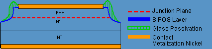
The exposed p-n junction surface is then passivated in a two-layer process.
- First, an oxygen doped, Semi-Insulating Poly Crystalline Silicon (SIPOS) layer is deposited onto the silicon junction surface by Low Pressure Chemical Vapor Deposition (LPCVD) to stabilize the region.
- Second, a thick layer of fired - on, high temperature glass is deposited over the SIPOS layer and protects the junction from ambient contamination and mechanical damage.
The wafers are then masked with a photoresist film and the top (Anode) Contact Metallization Layer of sintered nickel is applied (see figure 1).
Figure 1. Cross Section of GPP Die
Note: This process is typical to our GPP rectifier die; however, particular processes and materials used may vary depending on the specific device. Please contact a Nanjing Incorporated Applications Engineer for more detailed information regarding a specific device.